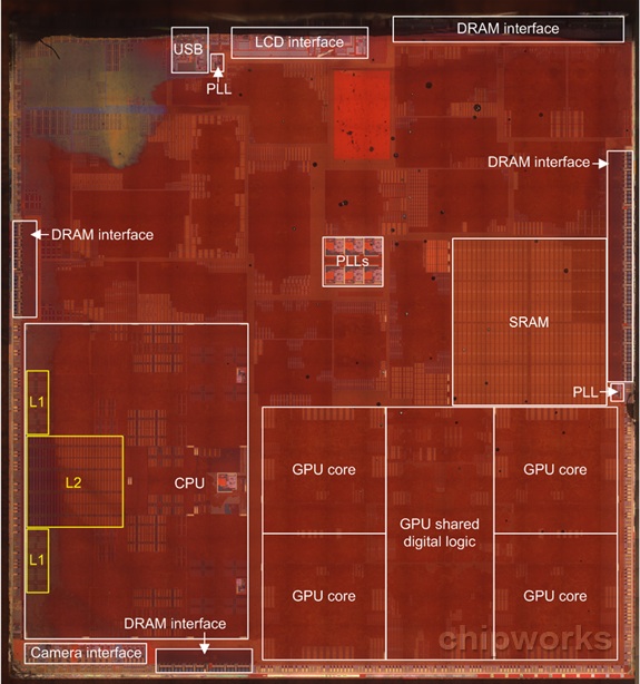
The firm has now had a chance to look at the A7's transistor die photo in detail and make a preliminary effort at identifying the various components of the chip. Chipworks stresses that the identifications are still tentative pending full circuit analysis, but that most of the identifications appear to make sense.
We publish this with the caveat that these are best guesses – we have not done any real circuit extraction to confirm them. The dual-core CPU and cache make up ~17% of the die area, and the quad-core GPU and shared logic about 22%. The CPU itself is not packed the same way as the A6 (see below), it looks much more like a conventional automated layout; although Linley Gwennap thinks that it’s still Apple designed, not the first ARM A53/57 usage.

The analysis identifies the CPU portion of the chip as being at the lower left of the image, with the quad-core graphics located at lower right. Previous work by AnandTech has identified the graphics as Imagination Technologies' PowerVR G6430 configuration, a member of the new "Rogue" series of GPUs from the company.
Also of interest is a large block of static RAM (SRAM) located along the right edge of the chip just above the graphics cores. Chipworks says that based on its size it represents approximately 3 MB of storage and that it could be the "secure enclave" used to house data associated with the Touch ID fingerprint sensor found on the iPhone 5s. No equivalent SRAM block is included on the previous-generation A6 chip from Apple.
The A7 is otherwise a fairly standard chip compared to Apple's previous designs, measuring only slightly larger than the A6 but offering significantly greater performance.
via MacRumors: Mac News and Rumors - All Stories http://www.macrumors.com


